PAL’s R&D TEAM IN SEARCH OF PLATING ‘HOLY GRAILS’Several recessions ago, the British business guru Sir John Harvey-Jones said something along the following lines to an audience of businessmen and women who attended one of his Master Classes: “I bet you’re all feeling very proud of the fact that you have come through the recession and can be here today. However, just a word of warning --- more companies go under during the recovery from recession than do during it”. It’s true of course. When times are hard many companies make
severe cutbacks both in terms of CAPEX and OPEX and then, “Here at PAL we have not fallen into any traps of this sort…
far from it!” says Geoff Paterson. “One vital area in
which we most definitely have not cut back is investment in R&D.
Dr Paul Henington, who heads our New Technologies Department, and
his talented team have been working tirelessly in search of a variety
of plating “holy grails”. And over the past year we have
achieved some stunning results.” Quest - To successfully fill, by plating
techniques, blind vias, with increasing aspect ratios. Dr. Paul Henington explains the importance of via filling: “The
"Real Estate" of available area on HDI circuit boards
has been becoming increasingly critical. As tracks and lands fight
foravailable space, the only way to advance is to completely fill
microvias (usually blind vias) and then reuse the area over the
via as new Real Estate. Initial attempts to fill the vias with epoxy
resin during bonding gave rise to problems of air entrapment. Subsequently
there were successful attempts at filling the vias ”PAL started R and D work on 'via filling by electroplating' at the end of 2000, initially as a preparatory study. But in the last year we have moved on to carry out Laboratory scale tests, both in Hong Kong and at a customer's base. Just in time as it turns out. We had predicted that there would be interest from customers in Asia, as the technology has been most successfully applied in Japan up to now. But we have been encouraged by the number of enquiries from Taiwan and most recently Europe also. ”We are now in the advanced stages of planning with a number of chemistry suppliers on how to integrate their processes with our equipment. At the same time we have engineering staff with key customers, carrying out preparations for trial retrofit of their PAL lines to carry out via filling. We look forward to this becoming a key area of business in the near future.”
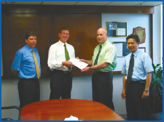
There were double celebrations at PAL in late June this year for not only had they just landed their first order for a plating line from Germany for some time, but the machine on order from RUWEL will be a record breaker, for it will be the widest that PAL has ever made. “It goes without saying that we are delighted to have received this order from the RUWEL group for a pattern plate machine with pulse plating, eductors and auto load/unload,” says Geoff Paterson, PAL’s Managing Director. “The new line, which will be housed in a specially built extension at the production site Geldern I at the RUWEL Headquarters in Geldern, will have a 5.75m wide tank, breaking our previous record by more than 50 cm, and is being designed to produce 19,000 panels each week. We will be delivering it in October and it will be fully commissioned by January/February 2003.” “We are impressed not only by PAL’s professionalism and engineering competence, but by the opinion of other users of PAL equipment,” explains Ad van der Kruijs, Member of the Executive Board of the RUWEL AG, responsible for technology. “Before making our final decision we saw PAL machines in operation at Aspocomp at Salo in Finland and TT Electronics (Prestwick Circuits) in Scotland. What we saw, and the comments made by the people in Finland and Scotland about the quality of plating and PAL’s after-sales service, helped us make our decision and we duly placed our order for the new line with PAL.” RUWEL is very firmly one of the major global players in the circuit board industry and a company with a long and distinguished history. It was founded in 1945 and initially produced capacitors. In 1956 they introduced the series-produced single-sided printed circuit to the market place – the first European company to do so. By 1957 the company was producing double-sided through hole PCBs and multilayer production began in 1961 – the rest, as they say, is history. RUWEL is justifiably proud of its position as one of the biggest circuit board manufacturers in Europe. The group now has seven highly specialised production plants in Germany and Denmark. “We pride ourselves on our ability to offer ‘One Stop Shopping’and ‘Single Sourcing’ to our customers,” says Ad van der Kruijs. “We offer virtually all types of boards for a wide range of technologies and in quantities ranging from development samples, to runs in their millions. We know how important it is to work with our customers to ensure that we produce exactly what they need – and we know that this is PAL’s business maxim too; it is this commonality of approach that is making for a productive relationship with PAL. Each of our plants specialises in particular areas. At our plant Geldern I, where the new PAL line will be installed, we have a workforce of 380 and manufacture up to eight layer multi layer PCBs with plated through holes in medium sized lots and in large quantities. We are very much looking forward to the new machine being in full production in the first quarter of 2003.” More on RUWEL at www.ruwel.de
|
||||
